Abstract
The physical and chemical properties of semiconductor materials change drastically when its size is reduced to nanoscale due to their large surface area or quantum size effect. Metal oxide (MOx) semiconducting nanostructures hold the potential for playing a critical role in the development of a new platform for renewable energies, including energy conversion and storage through photovoltaic effect, solar fuels, light-emitting nano devices, laser technology and water splitting. Further development of nanotechnology will certainly lead to significant breakthroughs in the semiconductor industry.
Keywords
Metal oxide (MONPs), Batteries, Antennas, Solar cells, Optoelectronics, IGT
Introduction
The variety of methods employed during the fabrication of MONPs can alter the characteristics and control the properties of the obtained nano-oxides [1-9]. The reaction mechanisms and, therefore, the functionality of nanostructured MOx depend on their composition, crystallographic structure, morphology, surface stoichiometry and geometry, interactions of the phases, etc. For achieving nanostructures with a set of desired properties, it is vital to summarize the existing information for variations in functional properties and characteristics of nanostructured MOx to expand our understanding beyond the existing knowledge. For that reason, this work was aimed at exploring the complications to induce further investigations by summarizing new techniques, benefitting the features of the MONPs and successful studies. The many varieties of techniques, types of nano-oxides, and combinations used just confirm the complexity of correlation between changes of nanostructure and composition on the one hand, and on the other hand, the resultant properties of the designed device. In recent years, dilute magnetic oxide semiconductors are finding much interest due to their important properties such as optical transmittance, electrical conductivity and ferromagnetism [10-13]. Semiconductor nanomaterials and devices are still in the research stage, but they are promising for applications in many fields, such as solar cells, nanoscale electronic devices, light-emitting diodes, laser technology, waveguide, chemical.
Properties of Nano-oxides
At present, nanoparticle research is an area of intense scientific activity due to a variety of potential applications in several fields [14]. The electronic structure of nanoparticles can reveal semiconductor, metallic, or insulator character. The unique chemical and physical properties of MONPs are attributed to the high density and limited size of corners and edges on their surface. Potential technological applications of metal oxide nanoparticles play a vital role attracting researchers with considerable interest from the fields of materials chemistry, medicine, agriculture, information technology, biomedical, optical, electronics, catalysis, environment, energy, and sense. Changes in cell parameters due to the size-related structural alterations have been observed, for example, in nanoparticles of CuO, ZnO, SnO2, Al2O3, MgO, ZrO2 AgO, TiO2, CeO2, etc.
As the size decreases in the nanoparticles, an increasing number of surface and interface atoms generates strain or stress and adjoining structural perturbations [15]. The specific size of the nanoparticle can alter magnetic, conducting, chemical, and electronic properties [16].
Classifications of Semiconductor Nanostructures
In nanocrystalline materials, the electrons are confined to regions having one, two or three dimensions (Figure 1) when the relative dimension is comparable with the de Broglie wavelength. For a semiconductor like CdSe, the de Broglie wavelength of free electron is around 10 nm. The nanostructures of semiconductor crystals having the z direction below this critical value (thin film, layer structure, quantum well) are defined as 2D nanostructures. When the dimension both in the x and z direction is below this critical value (linear chain structure, quantum wire) the nanostructures are defined as 1D and when the y direction is also below this threshold (cluster, colloid, nanocrystal, quantum dot) it is referred to as 0D.
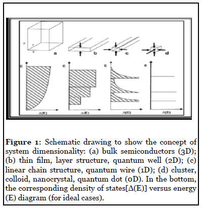
Figure 1: Schematic drawing to show the concept of system dimensionality: (a) bulk semiconductors (3D); (b) thin film, layer structure, quantum well (2D); (c) linear chain structure, quantum wire (1D); (d) cluster, colloid, nanocrystal, quantum dot (0D). In the bottom, the corresponding density of states[Δ(E)] versus energy (E) diagram (for ideal cases).
Semiconducting Ceramic Oxide Materials
Metal oxide semiconductors such as SnO2, ZnO, WO3, and TiO2 are wide-band-gap semiconductors and exhibit a change in electrical conductivity proportional to the composition of the gas surrounding them. Therefore, they are the popular and functional sensing materials for the production of inexpensive gas sensing devices (258).
Regarding these sensing materials, H2O is adsorbed on the oxide surface in molecular and hydroxyl forms. Water molecules increase the conductivity of n-type ceramics and decrease the conductivity of p-type ceramics. This observation has been explained as the donation of electrons from the chemically adsorbed water molecules to the ceramic surface. An alternative explanation suggested that the water molecules replace the previously adsorbed and ionized oxygen (O−, O2−, etc.) and consequently discharge the electrons from the ionized oxygen. Therefore, the ‘donor effect’ could result from both. The surface concentration of electrons causes the conductivity, and this style of sensing is typically called ‘electronic type.’ On the other hand, physically adsorbed water layer may be relatively proton-conductive. It is because of this observation that we conclude that the conductivity of ceramic semiconducting materials is due to the addition of both electrons and protons (ionic) at room temperature. However, at high temperatures (>100°C) moisture cannot effectively condense on the surface. Hydrogen atoms contact the material surface (predominantly at the oxygen sites) and attract electrons. A depletion region forms initially due to adsorbed oxygen and the liberated electrons may counteract the depletion. As already stated, adsorbed water molecules increase the conductivity of n-type ceramic semiconductors, therefore practically all the published research reports on n-type ceramics.
Nanoparticles Synthesis Methods
Wet chemical methods
The drive for miniaturization with the corresponding demand for smaller machines and components using less resources and energy that occurred during the last two decades, have been rapidly pushing the industry to the atomic and nanometer scale. The development of new synthesis strategies for advanced materials with enhanced properties and affording an effective control at the nanometer level is therefore required. Amongst the available synthetic methods employed for the development of nanosized systems, there are two main general approaches: “bottom-up” and “top-down”. The former applies to the creation of organic and inorganic structures, atom-by-atom or molecule-by-molecule. It implies the use of atoms or molecules as building blocks, to design and assemble nano arrangements of atoms in a functional form to give macroscopic systems. The concept of ‘organic–inorganic hybrid’ materials emerged very recently with the birth of ‘soft’ inorganic chemistry processes, particularly the solvothermal / hydrothermal and sol–gel process which is probably the supreme soft inorganic chemistry process, allowing a tailored chemical design [2-4] . The unique low temperature processing characteristics of this process allow the chemical design of organic–inorganic hybrid materials through the incorporation of low molecular weight organic molecules with appropriate functionalities into inorganic moieties, at temperatures at which the organic ones are not destroyed.
It is in the design and characterization of advanced materials, that the importance of new interdisciplinary studies may be realized. Thus, for the design of novel advanced functional nanomaterials, the uniformity of the shape and size of the nanoparticles is a key issue. NC samples must be monodisperse in terms of size, shape, internal structure and surface chemistry. Nanoparticles are considered monodisperse when their size distribution is < 5%. In the past decade, a particular interest was taken in the development of new synthetic routes, enabling the rigorous control of the morphology and size of the nanoparticles. The preparation of nanoparticles can be achieved through different approaches, either chemical or physical, including gaseous, liquid and solid media. While physical methods generally tend to approach the synthesis of nanostructures by decreasing the size of the constituents of the bulk material (top-down approach), chemical methods tend to attempt to control the clustering of atoms/molecules at the nanoscale range (bottom-up approach) Figure 2. However, the wet chemical methods are the most popular, because they present several major advantages over the other conventional methods, i.e., they are highly reliable and cost effective, allow a much more rigorous control of the shape and size of the nanoparticles and the agglomeration of the resulting particles can be alleviated by functionalization with different capping ligands [17]. The wet chemical synthesis routes offer an easy way to yield colloidal solutions with a large range of particle sizes on the gram scale in combination with high reproducibility. The following wet chemical methods have been successfully employed for developing different types of nanoparticles: 1. Sol-Gel 2. Solvothermal/hydrothermal 3. Co-precipitation.
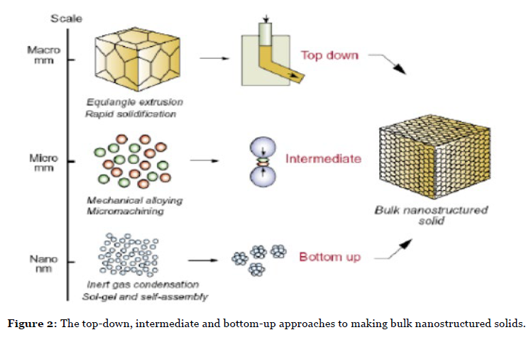
Figure 2: The top-down, intermediate and bottom-up approaches to making bulk nanostructured solids.
Surface Modification of Nanocrystals and Interparticle Forces in Solution
To produce well-defined 2D and 3D superlattices of nanocrystals, highly stable materials are needed. Furthermore, various forces have to be taken into account. Let us first list the various parameters involved in nanocrystal self-assemblies. Due to Van der Waals interactions, particles in the nanometer-size range have a strong tendency to agglomerate (Figure 3). It is therefore important to develop synthetic methods by which the particles can be stabilized, i. e., where repulsive and attractive forces between particles balance each other mainly electrostatic and steric forces that prevent agglomeration of nanoparticles. Electrostatic stabilization involves the creation of an electrical double layer arising from ions adsorbed on the surface and the associated counter ions that surround the particle. Thus, if the electric potential associated with the double layer is sufficiently high, the Coulomb repulsions between the particles prevent their agglomeration (Figure 4). Steric stabilization is achieved by the adsorption of organic molecules containing suitable functional groups, such as –SH, –COOH and –NH2, at the particle surface. Indeed, the lengths of the alkyl chains are usually greater than the range over which the forces of attraction between nanocrystals are active. In addition, dipolar magnetic interactions are to be taken into account for singledomain magnetic nanocrystals.
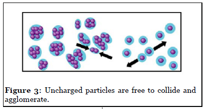
Figure 3: Uncharged particles are free to collide and agglomerate.
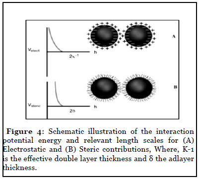
Figure 4: Schematic illustration of the interaction potential energy and relevant length scales for (A) Electrostatic and (B) Steric contributions, Where, K-1 is the effective double layer thickness and δ the adlayer thickness.
Semiconductor nanomaterials have interesting physical and chemical properties and useful functionalities, when compared with their conventional bulk counterparts and molecular materials. Narrow and intensive emission spectra, continuous absorption bands, high chemical and photobleaching stability, processability, and surface functionality are among the most attractive properties of these materials. The development of “nanochemistry” is reflected in an immense number of publications on the synthesis of semiconductor nanoparticles [18]. For instance, the spatial quantum confinement effect results in significant change in optical properties of semiconductor nanomaterials. The very high dispersity (high surface-to-volume ratio), with both physical and chemical properties of the semiconductor has a major influence on their optical and surface properties. As a result, semiconductor nanomaterials have been the focus of research for about 20 years and have attracted significant interest in research and applications in diverse disciplines such as solid-state physics, inorganic chemistry, physical chemistry, colloid chemistry, materials science, and recently biological sciences, medical sciences, engineering, and interdisciplinary fields. Among the unique properties of nanomaterials, the movement of electrons and holes in semiconductor nanomaterials is primarily governed by the well-known quantum confinement, and the transport properties related to phonons and photons are largely affected by the size and geometry of the materials [19-22]. The specific surface area and surface-to-volume ratio increase drastically as the size of the material decreases [19,23]. Parameters such as size, shape, and surface characteristics can be varied to control their properties for different applications of interest [24]. These novel properties of semiconductor nanomaterials have attracted significant attention in research and applications in emerging technologies such as nanoelectronics, nanophotonics, energy conversion, non-linear optics, miniaturized sensors and imaging devices, solar cells, catalysis, detectorsphotography biomedicine etc., In this section we discuss the application of semiconductor nanomaterials in catalysis and me.
Semiconductor Nanomaterials for Hydrogen Production
The extensive use of fossil fuel over the last 150 years has caused a rise in urban ill-health, economic dependence, political unrest and many cases of warfare [25]. A recent European study revealed that more deaths are caused by car emissions than by car accidents [26], and a parallel Swedish study reported that pollution can increase the risk of having cancer by 40-70 % [27] and recent atmospheric investigations have also shown a substantial increase in the concentrations of carbon oxide and other greenhouse gases, with potentially threatening consequences to the global climate. Growing environmental concerns are related to the extensive use of non-sustainable fossil fuels (oil, natural gas and coal) and a constantly increasing energy demand for clean and sustainable sources of energy. Hydrogen is a promising alternative fuel, since it is completely pollution-free and can readily be produced from renewable energy resources, thus eliminating the net production of greenhouse gases. Recent studies have indicated that hydrogen fuel costs are reasonable and hydrogen is therefore an ideal candidate to replace fossil fuels as an energy carrier. The production of hydrogen from liquid hydrocarbon fuels and adsorption on various solids including carbon has attracted a lot of attention by the media and the automotive industry. There is increasing environmental pollution, caused by combustion engines, and additional problems associated with large-scale mining, transportation, processing and usage of fossil fuel. Photocatalysis is expected to make a great contribution to both environmental treatment (emission cleaning and water purification) and renewable energy. Hydrogen (H2) is widely considered to be the future clean energy carrier in many applications, such as environmentally friendly vehicles, domestic heating, and stationary power generation. Photocatalytic hydrogen production from water in one of the promising techniques due to the following advantages: It is based on photon (or solar) energy, which is a clean, perpetual source of energy, and mainly water, which is a renewable resource. It is an environmentally safe technology without undesirable by-products and pollutants. The photochemical conversion of solar energy into a storable form of energy, i.e. hydrogen, allows one to deal with the intermittent character and seasonal variation of the solar influx. However, it requires a photocatalyst that should possess chemical stability, corrosion resistance, visible light harvesting and suitable band edges. The structural and electronic properties of semiconductor photocatalysts largely determine the process of photocatalytic H2 production, including basic steps such as the absorption of photons, charge separation and migration, and surface reactions.
Conclusion
Semiconductor nanomaterials are advanced materials for various applications, which have been discussed at length. The unique physical and chemical properties of semiconductor nanomaterial make it suitable for application in emerging technologies, such as nanoelectronics, nanophotonics, energy conversion, nonlinear optics, miniaturized sensors and imaging devices, solar cells, detectors, photography and biomedicine. There are three key steps in the development of nanoscience and nanotechnology: materials preparation, property characterization and devices fabrication. The preparation of nanomaterials is being advanced by numerous physical and chemical techniques. The purification and size selected techniques developed can produce nanocrystals with well-defined structure and morphology.CORMs/CO both have feature of exhibiting the re-endothelialization affected by wire-trauma injury [23].
In summary, small concentration of CO is vital for different therapeutic purposes. Indirect inhalation is the appropriate choice for the CO drug administration. CORMs and CORMats are the two subcategories of indirect inhalation. For carbonyl complexes, organometallic element is the key component. Organometallic complexes are good for carbonyl reaction, unfortunately it is involved in toxicity. To some extent, different techniques are applied to overcome this dilemma. Tissue selectivity and cytotoxic effects are also prime objective of drug development.
Acknowledgments
We are very grateful to the children, families and school staff, who kindly took part in this research.
References
2. Abu-Dief AM, Abdelbaky MS, Martínez-Blanco D, Amghouz Z, García-Granda S. Effect of chromium substitution on the structural and magnetic properties of nanocrystalline zinc ferrite. Materials Chemistry and Physics. 2016 May 1;174:164-71.
3. MAEAAA ER, Abu-Dief AM, El-Khatib RM. A robust Synthesis and Characterization for Superparamagnetic CoFe2O4 Nanoparticles as an Efficient and Reusable Catalyst for Green Synthesis of Some Heterocyclic Rings. Appl. Organometal. Chem. 2016;30:1022-9.
4. Abu-Dief AM, Nassar IF, Elsayed WH. Magnetic NiFe2O4 nanoparticles: efficient, heterogeneous and reusable catalyst for synthesis of acetylferrocene chalcones and their anti-tumour activity. Applied Organometallic Chemistry. 2016 Nov;30(11):917-23.
5. Abu-Dief AM, Mohamed WS. α-Bi2O3 nanorods: synthesis, characterization and UV-photocatalytic activity. Materials Research Express. 2017 Mar 29;4(3):035039.
6. Al-Saeedi SI, Abdel-Rahman LH, Abu-Dief AM, Abdel-Fatah SM, Alotaibi TM, Alsalme AM, Nafady A. Catalytic oxidation of benzyl alcohol using nanosized Cu/Ni schiff-base complexes and their metal oxide nanoparticles. Catalysts. 2018 Oct;8(10):452.
7. Mohamed WS, Abu-Dief AM. Synthesis, characterization and photocatalysis enhancement of Eu2O3-ZnO mixed oxide nanoparticles. Journal of Physics and Chemistry of Solids. 2018 May 1;116:375-85.
8. Mohamed WS, Alzaid M, SM Abdelbaky M, Amghouz Z, García-Granda S, M Abu-Dief A. Impact of Co2+ Substitution on Microstructure and Magnetic Properties of CoxZn1-xFe2O4 Nanoparticles. Nanomaterials. 2019 Nov;9(11):1602.
9. Toyos-Rodríguez C, Calleja-García J, Torres- Sánchez L, López A, Abu-Dief AM, Costa A, Elbaile L, Crespo RD, Garitaonandia JS, Lastra E, García JA. A Simple and Reliable Synthesis of Superparamagnetic Magnetite Nanoparticles by Thermal Decomposition of Fe (acac) 3. Journal of Nanomaterials. 2019;2019.
10. Ibrahim EM, Abu-Dief AM, Elshafaie A, Ahmed AM. Electrical, thermoelectrical and magnetic properties of approximately 20-nm Ni-Co-O nanoparticles and investigation of their conduction phenomena. Materials Chemistry and Physics. 2017 May 1;192:41-7.
11. Ibrahim EMM, Abdel-Rahman LH, Abu-Dief AM, Elshafaiea A, Kamel Hamdan S, Ahmed AM. Materials Research Bulletin. 2018;107:492–497.
12. Ibrahim EM, Abdel-Rahman LH, Abu-Dief AM, Elshafaie A, Hamdan SK, Ahmed AM. The synthesis of CuO and NiO nanoparticles by facile thermal decomposition of metal-Schiff base complexes and an examination of their electric, thermoelectric and magnetic Properties. Materials Research Bulletin. 2018 Nov 1;107:492-7.
13. Abdel Rahman LH, Abu-Dief AM, El-Khatib RM, Abdel-Fatah SM, Adam AM, Ibrahim EM. Sonochemical synthesis, structural inspection and semiconductor behavior of three new nano sized Cu (II), Co (II) and Ni (II) chelates based on tri-dentate NOO imine ligand as precursors for metal oxides. Applied Organometallic Chemistry. 2018 Mar;32(3):e4174.
14. Taylor R, Coulombe S, Otanicar T, Phelan P, Gunawan A, Lv W, Rosengarten G, Prasher R, Tyagi H. Small particles, big impacts: a review of the diverse applications of nanofluids. Journal of applied physics. 2013 Jan 7;113(1):1.
15. Bansal V, Poddar P, Ahmad A, Sastry M. Roomtemperature biosynthesis of ferroelectric barium titanate nanoparticles. Journal of the American Chemical Society. 2006 Sep 13;128(36):11958-63.
16. Liu WT. Nanoparticles and their biological and environmental applications. Journal of bioscience and bioengineering. 2006 Jul 1;102(1):1-7.
17. Cushing BL, Kolesnichenko VL, O’Connor CJ. Recent advances in the liquid-phase syntheses of inorganic nanoparticles. Chemical reviews. 2004 Sep 8;104(9):3893-946.
18. Eychmüller A. Aerogels from semiconductor nanomaterials. Angewandte Chemie International Edition. 2005 Aug 5;44(31):4839-41.
19. Alivisatos AP. Perspectives on the physical chemistry of semiconductor nanocrystals. The Journal of Physical Chemistry. 1996 Aug 1;100(31):13226-39.
20. Alivisatos AP. Semiconductor clusters, nanocrystals, and quantum dots. science. 1996 Feb 16;271(5251):933-7.
21. Burda C, Chen X, Narayanan R, El-Sayed MA. Chemistry and properties of nanocrystals of different shapes. Chemical reviews. 2005 Apr 13;105(4):1025-102.
22. Murray CB, Kagan AC, Bawendi MG. Synthesis and characterization of monodisperse nanocrystals and close-packed nanocrystal assemblies. Annual review of materials science. 2000 Aug;30(1):545-610.
23. Chen X, Lou Y, Dayal S, Qiu X, Krolicki R, Burda C, Zhao C, Becker J. Doped semiconductor nanomaterials. Journal of nanoscience and nanotechnology. 2005 Sep 1;5(9):1408-20.
24. Li J, Zhang JZ. Optical properties and applications of hybrid semiconductor nanomaterials. Coordination Chemistry Reviews. 2009 Dec 1;253(23-24):3015-41.
25. AQMD. Smog and Health. The south coast air quality management district. http://www.Aqmd.gov/ smog/inhealth.html. Accessed 1996.
26. Sheethaler R. Synthesis report on health costs due to road traffic-related air pollution-an impact assessment project Austria, France and Switzerland. WHO Regional office for Europe. 1999.
27. Altmann M. World health organization: more deaths caused by car emissions than by accidents. Hydrogen-Gazette june 22.