Commentary
Recently, our group published a review about surface enhanced Raman scattering (SERS) in SmartMat, which summarized the recent developments of noble metal and semiconductor SERS substrates, and then proposed the key factors for substrate design and future directions. The fundamental theories for SERS technique, i.e., the electromagnetic enhancement mechanism and chemical enhancement mechanism, and the design strategies for noble metal and semiconductor substrates are introduced detailed.
Raman spectrum is the fingerprint spectrum of molecular vibration, where different molecules present different vibration frequencies, so it is an important technique for substance identification [1,2]. The position, intensity, shape, and the half-height width of the Raman peak are all important information for identifying chemical bonds, functional groups, crystallinity and strain. However, the low intensity of Raman spectroscopy resulted in its sluggish developed for a long time after discovery, until the high-quality Raman spectrum of monolayer pyridine molecules adsorbed on the surface is obtained by Fleischmann et al. in 1974 [3]. Since then, Raman spectroscopy has developed rapidly and has been used in many fields, such as trace detection, biological sensing, situ analytical chemistry, and electrochemical. However, SERS substrate material still faces many shortcomings, such as the sensitivity and selectivity, which are two important parameters in practical applications. Considerable efforts have been made by researchers to design high-sensitive and selective SERS substrates ranging from noble metals to semiconductor [4–6], as shown in Figure 1.
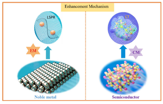
Figure 1. Diagram for the enhancement mechanism of SERS.
SERS-active substrates mainly include noble metals and semiconductor substrate, depending on the electromagnetic (EM) field enhancement and chemical (CM) enhancement respectively, as shown in Figure 1. Localized surface plasmon resonance (LSPR) and hot spot are the main reasons for EM enhancement of noble metal substrates, which usually occurs at the sharp tips, corners and nanogaps of nanostructure. Therefore, nanostructures with abundant sharp tips or corners are designed to realize the excellent SERS activity [7], i.e., nanoflowers [8], nanostar [9], dendritic [10], nanotriangles [11], nanotriangles and hedgehog, where the sharp tips can concentre charges at the sharp tips, edges or corners due to the lightning rod effect and lead to strong LSPR at local positions [12]. In addition, the “hot spot”, nanogaps between nanoparticles, can effectively amplify the electric field and enhance the Raman signal. 1D hot spots in dimer, 2D hot spot in the ordered array, and 3D hot spot in a droplet of citrate- Ag sols or superlattice have been introduced in detail, and the influence of gap size, density and spatial distribution on SERS performance was also introduced. For gold nanorods, it is proved that end-to-end assembly will produce a strong SERS enhancement which have been used in biosensing and contaminant detection [13,14]. Uniform and large-scale hot spot (>1cm2) for quantitative SERS at the single-molecule scale is realized by assembling of 6 nm-diameter AgNP [15]. Self-assembled 3D noble metal nanostructure could improve the SERS activity by increasing a large number of hot spots, for which the basic principles and design rules of optimal spatial distribution are introduced in detail by García-Lojo [16,17]. In addition, precise controlling of nanogaps can effectively locate hot spots and enrich molecules, which can promote quantitative analysis. By optimizing the design of the substrate material, single molecule detection has been achieved by noble metals substrates, however, it is expensive, unstable and no selectivity, so it is difficult to achieve quantitative detection. Das et al. successfully fabricated Au nanorods with tunable morphology by the seed-mediated growth approach, in which the aspect ratio of the Au NRs can be tuned by controlling the amount of Ag+, CTAB, AA, and seed particles. In addition, Au nanorods presented efficient SERS and SERRS performances under the excitation of 532 nm due to the synergistic effect of LSPR and molecular resonance [18].
The selectivity of semiconductor is better than the noble metal substrates, however, the intensity of SERS signal is lower which limit its further development. Therefore, how to boost the intensity of semiconductor substrates has been a research hotspot in recent years. This review introduced the latest development of chemical mechanism and the design of semiconductor substrates. Photo-induced charge transfer (PICT) mechanism is regarded as the main reason for CM. The quantitative description of charge transfer proposed by Lombardi et al. is very important for the theoretical study of enhancement mechanism [19,20], by which the coupling effect between LSPR and PICT can be researched clearly. For the design of semiconductor substrates, defect engineering and doping strategy are the common ways to enhance charge transfer between substrate and molecule by introducing new defect levels. The flat surface of two-dimensional semiconductor nanomaterials is helpful to determine the adsorption morphology of molecules on the substrate surface, which is convenient to study the interaction between substrate and adsorption molecules. We introduced the recent development of two-dimensional semiconductor substrates including graphene and h-BN, and the bifacial Raman enhancement is analyzed in detail. In addition, amorphous SERS substrate materials have been rapidly developed since our research group reported the porous amorphous ZnO naocages with excellent SERS performance [21]. Except for the amorphous ZnO naocages and TiO2 nanosheet, the amorphous molybdenum oxide quantum dots (HxMoO3) also present a strong SERS performance [22]. However, the enhancement mechanism of amorphous substrates needs further investigation.
Certainly, semiconductors and noble metal substrates have their own advantage and disadvantage to some extent. This review helps readers to further understand the enhancement mechanism and the current development status of SERS substrates, and then puts forward future research directions. Considering the respective advantages of noble metal and semiconductor substrates, the development of a new composite SERS-active substrate with large enhancement factor and selective recognition is of great significance to the future development of SERS technology.
Acknowledgements
This project is supported by the National Natural Science Foundation of China (52022006, 21875008, 51876008, and 51801007) and Beijing Natural Science Foundation (3202020).
References
2. Khan TM, Khan SU, Khan SU, Ahmad A, Abbasi SA, Khan EM, et al. Silver nanoparticle films by flowing gas atmospheric pulsed laser deposition and application to surface‐enhanced Raman spectroscopy. International Journal of Energy Research. 2020 Nov;44(14):11443-52.
3. Fleischmann M, Hendra PJ, McQuillan AJ. Raman spectra of pyridine adsorbed at a silver electrode. Chemical Physics Letters. 1974 May 15;26(2):163-6.
4. Khan TM, Mujawar MA, Siewerska KE, Pokle A, Donnelly T, McEvoy N, et al. Atmospheric pulsed laser deposition and thermal annealing of plasmonic silver nanoparticle films. Nanotechnology. 2017 Oct 4;28(44):445601.
5. Khan TM, Mujawar MA, Siewerska KE, Pokle A, Donnelly T, McEvoy N, et al. Atmospheric pulsed laser deposition and thermal annealing of plasmonic silver nanoparticle films. Nanotechnology. 2017 Oct 4;28(44):445601.
6. Khan TM, Lunney JG, O’Rourke D, Meyer MC, Creel JR, Siewierska KE. Various pulsed laser deposition methods for preparation of silversensitised glass and paper substrates for surface-enhanced Raman spectroscopy. Applied Physics A. 2019 Sep;125(9):1-7.
7. Liu L, Wu Y, Yin N, Zhang H, Ma H. Silver nanocubes with high SERS performance. Journal of Quantitative Spectroscopy and Radiative Transfer. 2020 Jan 1;240:106682.
8. Ye S, Benz F, Wheeler MC, Oram J, Baumberg JJ, Cespedes O, Christenson HK, et al. One-step fabrication of hollow-channel gold nanoflowers with excellent catalytic performance and large singleparticle SERS activity. Nanoscale. 2016;8(32):14932-42.
9. Nehra K, Pandian SK, Bharati MS, Soma VR. Enhanced catalytic and SERS performance of shape/size controlled anisotropic gold nanostructures. New Journal of Chemistry. 2019;43(9):3835-47.
10. Cheng ZQ, Li ZW, Yao R, Xiong KW, Cheng GL, Zhou YH, et al. Improved SERS performance and catalytic activity of dendritic Au/ Ag bimetallic nanostructures based on Ag dendrites. Nanoscale Research Letters. 2020 Dec;15(1):1-7.
11. Tian X, Zong J, Zhou Y, Chen D, Jia J, Li S, et al. Designing caps for colloidal Au nanoparticles. Chemical Science. 2021;12(10):3644-50.
12. Pan S, Sahu BK, Amirthapandian S, Dhara S, Das A. Growing AuNRs in a single step with NIR plasmon for superior SERS and plasmonic photothermal performance. Journal of Physics and Chemistry of Solids. 2022 Feb 1;161:110421.
13. Lee A, Ahmed A, Dos Santos DP, Coombs N, Park JI, Gordon R, et al. Side-by-side assembly of gold nanorods reduces ensembleaveraged SERS intensity. The Journal of Physical Chemistry C. 2012 Mar 8;116(9):5538-45.
14. Abtahi SM, Burrows ND, Idesis FA, Murphy CJ, Saleh NB, Vikesland PJ. Sulfate-mediated end-to-end assembly of gold nanorods. Langmuir. 2017 Feb 14;33(6):1486-95.
15. Chen HY, Lin MH, Wang CY, Chang YM, Gwo S. Large-scale hot spot engineering for quantitative SERS at the single-molecule scale. Journal of the American Chemical Society. 2015 Oct 28;137(42):13698- 705.
16. García-Lojo D, Núñez-Sánchez S, Gómez-Graña S, Grzelczak M, Pastoriza-Santos I, Pérez-Juste J, et al. Plasmonic supercrystals. Accounts of chemical research. 2019 Jun 25;52(7):1855-64.
17. García‐Lojo D, Modin E, Gómez‐Graña S, Impéror‐Clerc M, Chuvilin A, Pastoriza‐Santos I, et al. Structure and Formation Kinetics of Millimeter‐Size Single Domain Supercrystals. Advanced Functional Materials. 2021 Apr 22:2101869.
18. Sahu BK, Dwivedi A, Pal KK, Pandian R, Dhara S, Das A. Optimized Au NRs for efficient SERS and SERRS performances with molecular and longitudinal surface plasmon resonance. Applied Surface Science. 2021 Jan 30;537:147615.
19. Lombardi JR, Birke RL. A unified view of surface-enhanced Raman scattering. Accounts of Chemical Research. 2009 Jun 16;42(6):734-42.
20. Lombardi JR, Birke RL. A unified approach to surface-enhanced Raman spectroscopy. The Journal of Physical Chemistry C. 2008 Apr 10;112(14):5605-17.
21. Wang X, Shi W, Jin Z, Huang W, Lin J, Ma G, et al. Remarkable SERS activity observed from amorphous ZnO nanocages. Angewandte Chemie. 2017 Aug 7;129(33):9983-7.
22. Li H, Xu Q, Wang X, Liu W. Ultrasensitive surface‐enhanced Raman spectroscopy detection based on amorphous molybdenum oxide quantum dots. Small. 2018 Jul;14(28):1801523.