Abstract
Graphene is often referred to as bi-, tri- or few-layered (4 to 10 layers), despite it being single-layered. Two commercial graphite samples (G and GE) and three commercial graphene samples (G1, G2, and G3) were characterized by Raman spectroscopy, scanning electron microscopy, X-ray diffractometry and atomic force microscopy. The structural similarities and differences between graphite and graphene were compared with literature information. A mixture of hexagonal (2H) and rhombohedral (3R) phases were identified in samples G1, G2, G3, and GE by X-ray diffraction. Graphene is observed to differ from graphite-based on Raman spectroscopic studies at room temperature. Atomic force microscopy on graphene films at 514 nm radiation showed ~ 3, 7, and 9 layers for G1, G2, and G3, respectively.
Keywords
Graphene; Graphite; Crystal structure; Nanomaterials; Raman spectroscopy; Atomic force microscopy; X-ray diffractometry; Scanning electron microscopy
Introduction
The most important elemental-carbon-based materials include zero-, one-, two-, and three-dimensionalstructured fullerenes, carbon nanotubes, graphene, and graphite, respectively. These non-metallic carbon materials have properties that are similar to semiconducting metals [1-3].
Honeycomb hexagonal carbon atoms in graphite exist as crystalline hexagonal (2H) or rhombohedral (3R) phases. Carbon layers exist in an ABAB sequence in the commonly occurring 2H graphite structure with B layers shifted to a registered position relative to the A layers. The ABCABC stacking sequence in the 3R structure has C and B layers shifted by the same distance relative to the B and A layers, respectively [4]. Although highly ordered/ oriented graphite has a 2H hexagonal structure, a minor fraction of the 3R rhombohedral phase may remain in high-quality samples [5].
The discovery that the special allotrope of carbon, graphene, can be fabricated by using the scotch tape approach to produce a single layer of graphite, and the thinnest- and strongest-known material universally, led to an increase in its popularity [6]. Graphene is often termed bi-, tri-, or few-layered (4 to 10 layers). Two-dimensional graphene consists of a sp2-hybridized carbon monolayered sheet network of densely packed rhombohedral-arranged honeycomb hexagonal crystal lattices and contains up to a dozen shells [7,8]. Graphene’s properties make it suitable in a variety of applications, such as batteries, sensors, structural composites, functional inks, electron emission displays, catalyst supports, in the biomedical field, and potentially in other future research fields [1-3,8-16].
Four main methods have been proposed to produce different graphene materials: (i) mechanical cleavage, (ii) chemical/plasma exfoliation from natural graphite, (iii) chemical vapor deposition, and (iv) epitaxial growth on electrically insulating surfaces [2,3,8,11,17]. Graphene has been produced industrially by the cold-temperature, solution-based drop-and-cast approach, ultrahigh vacuum chemical vapor deposition, and role-to-role-type mass production [11].
Because graphite and graphene have similar structures, it is difficult to distinguish their differences through a single technique of characterization; multiple techniques are required. The aim of this work was to utilize a suite of standard characterization techniques in order to elucidate the nanostructures of graphene. We characterized two commercial graphite and three graphene samples using scanning electron microscopy, X-ray diffractometry, Raman spectroscopy, and atomic force microscopy. Their structural similarities and differences were compared with literature information.
Materials and Methods
Materials synthesis
Two commercial graphite samples (G, GE) and three commercial graphene samples (G1, G2, G3) with ≥ 98% purity were purchased from Advanced Graphene Technologies (Perth, Western Australia). These graphene samples were synthesized through chemical exfoliation from expandable natural graphite [18].
Scanning electron microscopy
The surface morphologies of graphene samples (G1, G2, and G3) were studied using a variable pressure field emission scanning electron microscope (TESCAN MIRA3 XMU VP-FESEM, John de Laeter Centre, Curtin University, Australia). Secondary electrons at a 5-KV acceleration voltage with a working distance of ~14 mm. Energy-dispersive X-ray spectroscopy (EDS) was used to analyze the elemental compositions of graphene qualitatively.
Raman spectroscopy
Raman spectra were collected on a Labram 1B dispersive Raman spectrometer at 632.8 nm excitation, 2 mW power, a 150 μm slit, 50× objective, 600 lines per mm diffraction grating, and a Peltier-cooled CCD detector at - 40°C. The sample collection time was 60 sec (10 sec for silicon). All Raman spectra were shifted by the same 520.7 wavenumbers to correct for the silicon peak.
X-ray diffraction
Samples were run on a powder diffractometer D8 Advance (Bruker AXS, Germany), with a copper Kα radiation source at 40kV and 40mA and a LynxEye detector. The diffraction data were collected at a 2-theta scan range of 7.5–90°, a step size of 0.015°, a time/step of 0.7 sec, and a total scan time of ~ 60 mins.
Atomic force microscopy
An atomic force microscope (Dimension Icon FastScan, TESPA-V2 probe, Bruker, California, USA) with a nominal spring constant of 42 N/m, the resonant frequency of 300 kHz was used in tapping mode to characterize the dimensions and thickness of graphene sheets. Before the measurements, graphene powders were initially sonicated in water to break up the nanoplatelets for uniform dispersion and then spin-coated on a mica substrate.
Results and Discussion
Microstructural imaging
The morphology of three (G1, G2, and G3) graphene samples, as revealed by scanning electron microscopy is shown in Figure 1. These samples exhibited a flake-like or layered structure of graphene nanoplatelets. Some graphene layers appeared to have been “lifted” from the surface, which is an indication of material exfoliation. The graphene layers appeared reasonably thick, which suggests that these materials are graphene nanoplatelets rather than single layers. The use of either transmission electron microscopy or atomic force microscopy is necessary to ascertain the existence of exfoliation and determination of the thickness nanoplatelets (i.e., number of graphene layers).
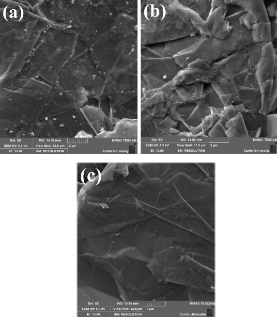
Figure 1. Scanning electron micrographs of graphene samples: (a) G1, (b) G2, and (c) G3.
Figure 2 shows a typical energy dispersive spectrum of graphene sample G3. Traces of elements, such as Al, Si, O, and Fe, are visible in the sample. Nonetheless, the graphene samples are of good quality with a purity above 98%.
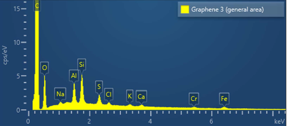
Figure 2. Energy dispersive spectrum of graphene sample G3 showing the presence of various trace elements.
Raman spectroscopy
Figure 3 shows the Raman spectra of two graphite and three graphene samples. The number of layers in graphene can be estimated from the intensity, shape, and position of the G and 2D bands. Whereas the 2D-band changes its shape, width, and position with an increase in the number of layers, the G-band peak position shows a down-shift with the number of layers. The characteristic peaks of graphene nanoplatelets can be seen in three bands, namely the G, D, and 2D bands at 1,578 cm-1, 1,334 cm-1, 2,679 cm-1, respectively. The vibration of sp carbon atoms yields the appearance of the G band as the primary characteristic band of graphene. The disordered vibrational peak of graphene is considered to ensue from the existence of a D band, which is applied to characterize structural defects in graphene samples [19]. Nanoplatelets of the graphene samples are well-defined with minimum defects present.
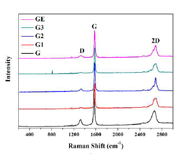
Figure 3. Raman spectra of graphite and graphene samples.
The difference in the two graphite samples is visible from their respective Raman spectra. The spectrum of graphite G appears to shift slightly to the left of graphite GE and has relatively broader peaks. This result suggests that graphite G has a finer particle size than graphite GE and a more disordered structure. The spectra in Figure 3 show that graphene samples G1–G3 were most likely synthesized from graphite GE rather than graphite G.
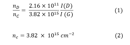
The concentration of Raman-active defects in ppm (parts per million) can be determined by taking the ratio of the defect density (nD) and the number of carbon atoms (nC) [20]:
Where I(D), and I(G) are the integration area of the D and G bands, respectively. Data in Figure 4 (a & b) show the integral area ratio, and the concentration defects for GE, and G graphite, and G1-G3 graphene samples, respectively. The measured I(D)/I(G) ratio for both G, and GE graphite samples are higher, thus indicating the defects are higher than in the G1-G3 graphene samples. Moreover, the defects of concentrations for G1, and G3 graphene samples are ~ 3 ppm, which are smaller than that for the G2 graphene sample (~ 10 ppm). A monolayer graphene generally exhibits no D band with the 2D band having a higher intensity than the G band [18]. Thus, the display of a weak D band in samples G1 and G3 indicates the presence of graphene with multilayers.
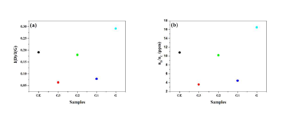
Figure 4. (a) Plot of integration area ratio I(D)/I(G) of the D and G bands, and (b) the concentrations defects for GE, and G graphite, and G1-G3 graphene samples.
X-ray diffraction
The diffraction patterns in Figure 5a show the crystalline structures of the two graphite and three graphene samples. The characteristic diffraction peaks of samples positioned at approximately 26.8°, and 55.0° correspond to the reflection of crystal planes (002) and (004), respectively. The former corresponds to an interlayer distance of 0.34 nm for (002) planes. It is noted that these peaks are quite broad for graphite sample G due to its smaller crystalline sizes and more disordered structure. In contrast, the graphene samples have sharp (002) and (004) peaks, thus indicating much larger crystallite sizes and well-ordered structures. Again, it can be observed that graphite G is quite different from graphite GE with a distinctive line-shift to the left at 26.8° and 55.0°. This line shift to lower angles for graphite G suggests the interlayer distance of (002) planes has increased due to its smaller crystallite size and a higher degree of disorder within the structure [21].
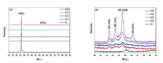
Figure 5. X-ray diffraction plots for graphite and graphene samples: (a) general view, and (b) expanded view at 2-theta = 40-50°.
Calculations of the apparent crystallite size (Lc) along the c-direction which will provide the information on the thickness of graphene nanoplatelets and thus the number of layers present. The number of graphene layers (Nc) along the c-axis can be calculated using the following equation [20]:
where Lc is the crystallite size along the c-direction, and d002 is the d-spacing for 2H (002) peak, which can be calculated from the following equations [20,22-24]:
where λ, β, θ, k is the X-ray wavelength of copper Kα radiation (0.154185 nm), line broadening at half the maximum intensity [full width at half maximum (FWHM)] of 2H (002) in radians, shape factor (0.91), and the Bragg angle, respectively.
Table 1 shows the calculated values of Lc and Nc for graphene samples (G1-G3). The multilayer nature of nanoplates in these samples is confirmed by the existence of 75 layers in G3, 101 layers in G2, and 102 layers in G1. These values are in good agreement with those obtained by Seehra and co-workers [20]. They calculated the values of Lc (22 - 37 nm) and the number of layers (65 – 109) for some commercial graphene materials from the analysis of XRD data.
| Graphene No. | 2θ (°) | FWHM (°) | Lc (nm) | d002 (nm) | Nc |
|---|---|---|---|---|---|
| G1 | 26.70 | 0.242 | 34.14 | 0.3339 | 102 |
| G2 | 26.71 | 0.243 | 34.00 | 0.3338 | 101 |
| G3 | 26.65 | 0.331 | 24.96 | 0.3345 | 75 |
Figure 5b shows the expanded view of the corresponding diffraction patterns at 2-theta = 40-50°. Several peaks corresponding to 2R and 3H phases can be observed. It is well known that graphene samples contain both phases [20,25]. Again, Seehra and co-workers [20] have analyzed the XRD data of 16 commercial graphene materials and observed the presence of 2R and 3H phases in them. The presence of the 3R structure is important for graphene materials since the 3R structure is a semiconductor with a tunable bandgap, and it is less stable than the 2H structure.
Atomic force microscopy
Images in Figure 6 (a-c) show the results of 3D atomic force microscopy and height profiles of three graphene samples (G1-G3). The layer thickness of graphene samples on the mica substrate was measured using NanoScope Analysis (version 1.0). The height differences of graphene G1, G2, and G3 are ~1.2 nm, ~2.4 nm, and ~2.8 nm, respectively. Single-layer graphene is a oneatom- thick planar sheet of carbon atoms that are packed in a dense honeycomb crystal lattice. Using AFM, the graphene layer thickness has been measured by several investigators to be in the range of 0.35–1 nm [26,27]. Similarly, graphene platelet thicknesses of ~0.6 nm and 1.0 - 1.6 nm have been measured by Park & Ruoff [17] and Novoselov et al. [6], respectively. Since the thickness of one single-layer graphene has a topographic height of ~0.335 nm, it follows that there are ~3, 7, and 9 graphene layers in samples G1, G2, and G3, respectively.
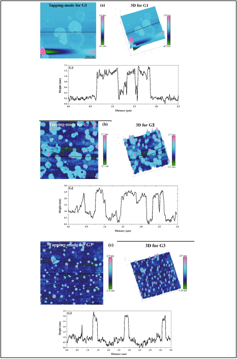
Figure 6. Images of 3D AFM and height profiles of spin-coated graphene on mica: (a) G1, (b) G2, and (c) G3. Note the color scale: green to pink where dark blue is mica, and light blue is spin-coated graphene. Measured height was indicated by the NanoScope Analysis software from the solid black line on the Tapping-mode of 3D AFM images.
The above-mentioned results of AFM and XRD imply that the sonication process and the subsequent spin-coating can break down the initial graphene nanoplatelets with 75-102 layers down to 3-9 layers via further exfoliation.
Conclusions
Graphene is a superior allotrope of carbon with a 2-D monolayered sheet network of sp2 hybridized carbon. A suite of standard characterization techniques was used to elucidate the nanostructures of graphene. Based on the results of SEM, Raman, XRD, and AFM analyses, it can be concluded that multilayered nanoplatelets are present in graphene samples G1-G3 with 75-102 layers. However, through a combination of sonication and spin-coating, these relatively thick nanoplatelets could be further broken down into thinner graphene films of 3-9 layers.
Acknowledgments
Prof. Mohindar Seehra of West Virginia University and Prof. Andrea Ferrari of Cambridge University kindly provided feedback on XRD and Raman results, respectively. The authors would like to thank Dr. Thomas Becker from Curtin University for assistance with the AFM measurements.
References
2. Kim H, Abdala AA, Macosko CW. Graphene/polymer nanocomposites. Macromolecules. 2010 Aug 24;43(16):6515-30.
3. Choi W, Lahiri I, Seelaboyina R, Kang YS. Synthesis of graphene and its applications: a review. Critical Reviews in Solid State and Materials Sciences. 2010 Feb 11;35(1):52-71.
4. Shi H, Barker J, Saidi MY, Koksbang R, Morris L. Graphite structure and lithium intercalation. Journal of Power Sources. 1997 Oct 1;68(2):291-5.
5. Zhou Z, Bouwman WG, Schut H, Pappas C. Interpretation of X-ray diffraction patterns of (nuclear) graphite. Carbon. 2014 Apr 1;69:17-24.
6. Novoselov KS, Geim AK, Morozov SV, Jiang D, Zhang Y, Dubonos SV, et al. Electric field effect in atomically thin carbon films. science. 2004 Oct 22;306(5696):666-9.
7. Latil S, Henrard L. Charge carriers in few-layer graphene films. Physical Review Letters. 2006 Jul 19;97(3):036803.
8. Rao CE, Sood AE, Subrahmanyam KE, Govindaraj A. Graphene: the new two-dimensional nanomaterial. Angewandte Chemie International Edition. 2009 Oct 5;48(42):7752-77.
9. A Guide to Graphene. https://www.azonano.com/ article.aspxArticleID=4841: Cheap Tubes Inc.; 2019.
10. Das TK, Prusty S. Recent advances in applications of graphene. International Journal of Chemical Sciences. 2013 Jan;4:39-55.
11. Kim H, Ahn JH. Graphene for flexible and wearable device applications. Carbon. 2017 Aug 1;120:244-57.
12. Wang L, Lee K, Sun YY, Lucking M, Chen Z, Zhao JJ, et al. Graphene oxide as an ideal substrate for hydrogen storage. ACS Nano. 2009 Oct 27;3(10):2995-3000.
13. Stoller MD, Park S, Zhu Y, An J, Ruoff RS. Graphene-based ultracapacitors. Nano Letters. 2008 Oct 8;8(10):3498-502.
14. Liu C, Alwarappan S, Chen Z, Kong X, Li CZ. Membraneless enzymatic biofuel cells based on graphene nanosheets. Biosensors and Bioelectronics. 2010 Mar 15;25(7):1829-33.
15. Balandin AA, Ghosh S, Bao W, Calizo I, Teweldebrhan D, Miao F, et al. Superior thermal conductivity of singlelayer graphene. Nano Letters. 2008 Mar 12;8(3):902-7.
16. Wang X, Zhi L, Müllen K. Transparent, conductive graphene electrodes for dye-sensitized solar cells. Nano Letters. 2008 Jan 9;8(1):323-7.
17. Park S, Ruoff RS. Chemical methods for the production of graphenes. Nature Nanotechnology. 2009 Apr;4(4):217.
18. Gu W, Zhang W, Li X, Zhu H, Wei J, Li Z, et al. Graphene sheets from worm-like exfoliated graphite. Journal of Materials Chemistry. 2009 May 21;19(21):3367-9.
19. Liu D, Dong Y, Liu Y, Ma N, Sui G. Cellulose Nanowhisker (CNW)/Graphene Nanoplatelet (GN) Composite Films With Simultaneously Enhanced Thermal, Electrical and Mechanical Properties. Frontiers in Materials. 2019;6:235.
20. Seehra MS, Geddam UK, Schwegler-Berry D, Stefaniak AB. Detection and quantification of 2H and 3R phases in commercial graphene-based materials. Carbon. 2015 Dec 1;95:818-23.
21. Babu VS, Seehra MS. Modeling of disorder and X-ray diffraction in coal-based graphitic carbons. Carbon. 1996 Jan 1;34(10):1259-65.
22. Abu-Dief AM, Mohamed WS. α-Bi2O3 nanorods: synthesis, characterization and UV-photocatalytic activity. Materials Research Express. 2017 Mar 29;4(3):035039.
23. Mohamed WS, Alzaid M, Abdelbaky MSM, Amghouz Z, García-Granda S, Abu-Dief AM. Impact of Co2+ Substitution on Microstructure and Magnetic Properties of CoxZn1-xFe2O4 Nanoparticles. Nanomaterials. 2019 Nov;9(11):1602.
24. Mohamed WS, Abu-Dief AM. Synthesis, characterization and photocatalysis enhancement of Eu2O3-ZnO mixed oxide nanoparticles. Journal of Physics and Chemistry of Solids. 2018 May 1;116:375-85.
25. Seehra MS, Narang V, Geddam UK, Stefaniak AB. Correlation between X-ray diffraction and Raman spectra of 16 commercial graphene–based materials and their resulting classification. Carbon. 2017 Jan 1;111:380-5.
26. Nemes-Incze P, Osváth Z, Kamarás K, Biró LP. Anomalies in thickness measurements of graphene and few layer graphite crystals by tapping mode atomic force microscopy. Carbon. 2008 Sep 1;46(11):1435-42.
27. Chen Z, Lin YM, Rooks MJ, Avouris P. Graphene nano-ribbon electronics. Physica E: Low-Dimensional Systems and Nanostructures. 2007 Dec 1;40(2):228-32.