Abstract
The article presents a commentary for the recent publication on nanocrytalline silicon thin films for heterojunction solar (SHJ) cells. The aim of the communication is to highlight some of the important mechanism discussed in the report for improved structure and interface properties which results in better device fill factor and hence enhanced efficiency. Furthermore, the discussion has been extended to present some of the recent literatures which have followed the similar guidelines for material synthesis with improved optical gain in applications of SHJ solar cells.
Keywords
Nanocrystalline silicon, Heterojunction solar cell, Silicon photovoltaic, Carrier selective layer
Introduction
Silicon photovoltaic has been one of the conventional topics of research interest from the past few decades to meet the requirement of clean and affordable energy. The commercialization of the silicon based photovoltaic device has now evolved with advanced designing. The focus of commercialization of the silicon photovoltaic in the last few decades is majorly aiming to achieve an inexpensive sustainable designing of the device. Silicon based heterojunction structures have attracted much scientific interest in terms of their potential characteristics and improved efficiency. Various combinations of stacked layers of doped and undoped thin film silicon were found to overcome some of the practical limitations of conventional designing of heterojunction solar cells in view of enhanced efficiency [1]. These factors are mainly associated with the unpassivated amorphous silicon thin film layer stacked in between the heterojunction cells. Several reports have demonstrated the effective replacement of amorphous layer with the crystalline thin layer. However, the thin crystalline layer is not similar to the bulk crystalline silicon though the structure is mainly identified as the modified morphology of the thin film amorphous silicon nearer to the transition zone during growth. These modified structural transformations may result in formation of embedded microcrystalline or nano-crystalline silicon depending on the size of the crystallite. The control over crystallite size could result in significant improvement in the material properties as well as the efficacy of the device. Other than potential characteristics for photovoltaics, the shape and size dependent applications of nanocrystallites have also been evolved in various fields for the production of nanostructured compounds for environment remediation, heterogeneous photocatalysts, multifunctional material, bioactive nanosurfaces, etc. [2-6].
The inclusion of nc-Si:H based stack in the heterojunction solar cell has been one of the advanced attractions for the designing of solar cell in view of exploring the suitable position of the layer to meet the necessary requirements of surface and interface layers. Recently the growth aspects and modified surface properties with the inclusion of nanocrystalline phase in the conventional a-Si:H thin films based layer for doped nano-crystalline/oxygen alloyed silicon (nc-Si:H/nc-SiO:H) thin film for heterojunction solar cells have been reviewed and compiled to report the advancement in the device structure based on the processing moderations [7]. The focus of the present commentary is to provide significant insights and to present the recent advancement in the doped nc-Si:H thin film based carrier selective layers for device applications. The attempt has been made to present a brief discussion for the advance designing of thin film silicon based heterojunction solar cells and the processing challenges for achieving the maximum fill factor and improved current densities. The article found to be informative for understanding various loss factors associated with the incorporation of thin film silicon layer and to address the solutions for limiting the existing junction and interface losses with the inclusion of nanocrystalline silicon thin films for heterojunction solar cells designing.
Background
Sharma et al. reports the limitations of power conversion efficiency with the both sides contacted a-Si:H/c-Si heterojunction solar cell due to short circuit current (Jsc) loss in order to address the modified architecture of the material [7]. The reported data compiled to provide a guide to analyze the significant loss factors due to device optics, i.e. parasitic loss, loss due to the refractive index mismatching, and electronic loss, i.e. loss due to defective sites which obstruct the dark conductivity (σdark). The significant role of embedded nanocrystallites in the amorphous phase led to enhance the optoelectronic properties of the material and hence improves the efficacy of solar cells with minimal current loss. In view of the mentioned considerations, the growth aspects of the materials were discussed to manage and meet the requirement of doped nc-Si:H thin films with thickness <10 nm while preserving the conductivities simultaneously with high doping [8]. The origin of crystallinity in the existing amorphous phase has been stated with the help of surface model considering the plasma interaction with the surface layer, and the growth zone model where the plasma interaction takes place at subsurface layer [9]. These structural modifications take place under specific plasma treatments during depositions or post depositions. Moreover, the evolution of embedded crystalline phase has also been the result of plasma discontinuity provided via pulsed plasma conditions [10,11].
The inclusion of nc-Si:H layer has been presented as one of the promising carriers’ selective layers for SHJ solar cells with improved optoelectronic properties. The material found significantly overcomes optical and electrical loss. Additionally, the alloying of nc-Si:H with oxygen results in modified refractive index and limiting parasitic loss when used as emitter. With the advantage of effective carrier transport the investigations for hole selective transport were also carried out by the researchers in order to explore the material and interface properties [1,12]. Figure 1 illustrates the potential improvements in the device structure with doped nc-Si:H/nc-Sio:H as carrier selective layer. The material suggested to have potential characteristics in terms of structural improvement when considered for the front and rare doped layers [13].
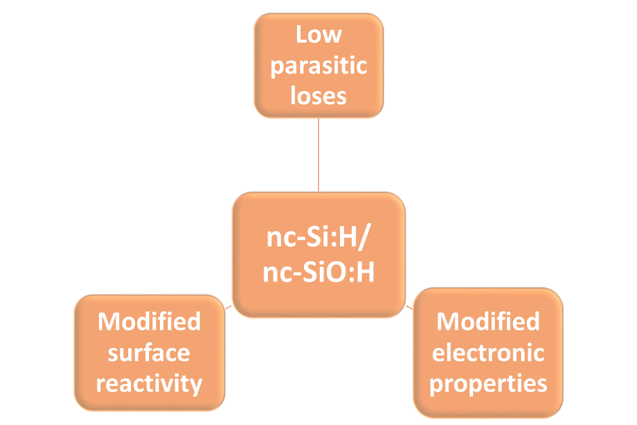
Figure 1. Advantages of nc-Si:H/nc-SiO:H thin film carrier selective layer for SHJ solar cells.
Discussion
In one of the recent studies the effective use of p-type nc-SiO-H based layer in stacked configuration with (p) nc-Si:H which exhibits a significant enhancement in the built-in potential at the interface has been presented [14]. The investigation using TCAD simulations highlights the important contribution of series resistance and hence the role of contact resistivity in improved transport mechanism. The thickness dependent activation energy Ea of the bi-layer was discussed to map its overall impact at the interface. An inverse relationship between the thickness and the activation energy of p-contact was suggested. Additionally, the hydrogen plasma interface treatment combined with very high frequency (VHF) was found to enhance the electrical properties significantly [15]. The p-contact stack was found to exhibit great effect on the distribution of hole transport laterally as well as vertically [14]. Solar cells with efficiency of 22.47 % were reported with an FF of 80%. The report also provides a theoretical understanding for the management of series resistance and role of hole transport in raising the electrical properties. It further highlights the similar transport characteristics improvements when the stacked device designing is considered as suggested by sharma [7].
Another challenge observed in application of doped nc-Si:H/nc-SiO:H layer is the attainability of high short circuit current density in view of managing the other surface and interfaces. Theoretically the highest observed value of FF has been reported to be 89.26% which is comparatively higher than the reported FF for the record efficiency solar cell i.e., 86.59% [16]. There is significant difference in the theoretical and experimental values which has been identified due to various factors including the contribution from series resistance and the unwanted recombination. The numerical approach has also been demonstrated in one of the recent reports to discuss the limitation in the attainment of FF [17]. These limitations were individually specified in view of auger recombination and bulk recombination with the presence of defective sites. To overcome such recombination loss factors the work has been explored further with the scope of improvements via correlating the ideality factor with various loss mechanisms which was not considered and discussed in the report of Sharma et al. The reported review was specific for underlining the experimental aspects of growth of nano-crystalline silicon and the surface modifications by suitable plasma techniques. Thus, the understanding of ideality factor correlation and based optimizations could be one of the suggested areas of research where the experimental aspects and the particle designing still be explored.
Conclusion
The article presents a commentary for the literature review on nc-Si:H thin films for SHJ solar cells which highlights most of the factors responsible for limiting the current and efficiency of solar cell in view of optical, carrier transport and contribution of crystallinity in the conduction and the surface passivation issues [7]. The mentioned review provides a guide to explore various aspects of nc-Si:H thin film based carrier selective layers for device application. A comparatively lower optical absorption with enhanced transparency was suggested with the inclusion of nc-SiO:H compared to a-Si:H as front carrier selective layer [1]. The embedded nanocrystallites are considered to be responsible for providing a conductive percolation path for conduction and thus to limit the transport barrier in conduction. The surface modification and restructuring via pre and post plasma treatments has also been considered to manage the growth barriers at the time of substitutional doping. The issue was also addressed in view of poor open circuit voltage (Voc) and device fill factor. Overall, the literature suggests the importance of thin (<5 nm) doped nc-Si:H carrier selective layer for front and rare contact layers grown under the specific plasma conditions to depict enhanced optical properties along with the transport benefits from the nanocrystalline phases [1]. However, the shortcoming of the cell designing with the suggested nc-Si:H found to have restrictions in terms of meeting the theoretical limits of the FF. The report demonstrated by Zhao provides significant insight to the advanced numerical approach in understanding the responsible factor in limiting current and highlights the role of various recombination mechanisms [14]. Additionally, suggestions have been made in terms of optimizing the value of ideality factor to overcome some of the significant recombination losses. The research is still open ended for providing critical growth aspects and further modification in view of enhanced current densities and hence good quality stable solar cell.
Author Contribution
Mansi Sharma: Visualization, conceptualization, writing original draft preparation, reviewing, editing.
Conflicts of Interest
There are no conflicts of interest.
References
2. Zinatloo-Ajabshir S, Morassaei MS, Salavati-Niasari M. Eco-friendly synthesis of Nd2Sn2O7–based nanostructure materials using grape juice as green fuel as photocatalyst for the degradation of erythrosine. Composites Part B: Engineering. 2019 Jun 15;167:643-53.
3. Zinatloo-Ajabshir S, Esfahani MH, Marjerrison CA, Greedan J, Behzad M. Enhanced electrochemical hydrogen storage performance of lanthanum zirconium oxide ceramic microstructures synthesized by a simple approach. Ceramics International. 2023 Dec 1;49(23):37415-22.
4. Moshtaghi S, Zinatloo-Ajabshir S, Salavati-Niasari M. Nanocrystalline barium stannate: facile morphology-controlled preparation, characterization and investigation of optical and photocatalytic properties. Journal of Materials Science: Materials in Electronics. 2016 Jan;27:834-42.
5. Pizzini S, Acciarri M, Binetti S, Cavalcoli D, Cavallini A, Chrastina D, et al. Nanocrystalline silicon films as multifunctional material for optoelectronic and photovoltaic applications. Materials Science and Engineering: B. 2006 Oct 15;134(2-3):118-24.
6. Yao L, Wang Y, Zhao J, Zhu Y, Cao M. Multifunctional nanocrystalline‐assembled porous hierarchical material and device for integrating microwave absorption, electromagnetic interference shielding, and energy storage. Small. 2023 Jun;19(25):2208101.
7. Sharma M, Panigrahi J, Komarala VK. Nanocrystalline silicon thin film growth and application for silicon heterojunction solar cells: a short review. Nanoscale Advances. 2021;3(12):3373-83.
8. Juneja S, Sudhakar S, Gope J, Lodhi K, Sharma M, Kumar S. Highly condcutive boron doped micro/ nanocrystalline silicon thin films deposited by VHF-PECVD for solar cell applications. J Alloys Compd. 2015;643:94-99.
9. Yang YH, Katiyar M, Feng GF, Maley N, Abelson JR. Subsurface hydrogenated amorphous silicon to μ c‐hydrogenated silicon transformation during magnetron
10. Watanabe Y, Shiratani M, Kubo Y, Ogawa I, Ogi S. Effects of low‐frequency modulation on rf discharge chemical vapor deposition. Applied Physics Letters. 1988 Oct 3;53(14):1263-5.
11. Hishida M, Sekimoto T, Matsumoto M, Terakawa A. Intermittent very high frequency plasma deposition on microcrystalline silicon solar cells enabling high conversion efficiency. Energies. 2016 Jan 13;9(1):42.
12. Haschke J, Messmer C, Cattin J, Bivour M, Boccard M, Ballif C. Injection-dependent lateral resistance in front-junction solar cells with nc-Si: H and a-Si: H hole selective contact. In2019 IEEE 46th Photovoltaic Specialists Conference (PVSC) 2019 Jun 16 (pp. 3042-3045). IEEE.
13. Bivour M, Schröer S, Hermle M, Glunz SW. Silicon heterojunction rear emitter solar cells: Less restrictions on the optoelectrical properties of front side TCOs. Solar Energy Materials and Solar Cells. 2014 Mar 1;122:120-9.
14. Zhao Y, Procel P, Han C, Mazzarella L, Yang G, Weeber A, et al. Design and optimization of hole collectors based on nc-SiOx: H for high-efficiency silicon heterojunction solar cells. Solar Energy Materials and Solar Cells. 2021 Jan 1;219:110779.
15. Zhao Y, Mazzarella L, Procel P, Han C, Yang G, Weeber A, et al. Doped hydrogenated nanocrystalline silicon oxide layers for high‐efficiency c‐Si heterojunction solar cells. Progress in Photovoltaics: research and applications. 2020 May;28(5):425-35.
16. Lin H, Yang M, Ru X, Wang G, Yin S, Peng F, et al. Silicon heterojunction solar cells with up to 26.81% efficiency achieved by electrically optimized nanocrystalline-silicon hole contact layers. Nature Energy. 2023 May;4:1-1.
17. Lin H, Wang G, Su Q, Han C, Xue C, Yin S, Fang L, Xu X, Gao P. Unveiling the mechanism of attaining high fill factor in silicon solar cells. Progress in Photovoltaics: Research and Applications. 2024.